Jumpers (JP)
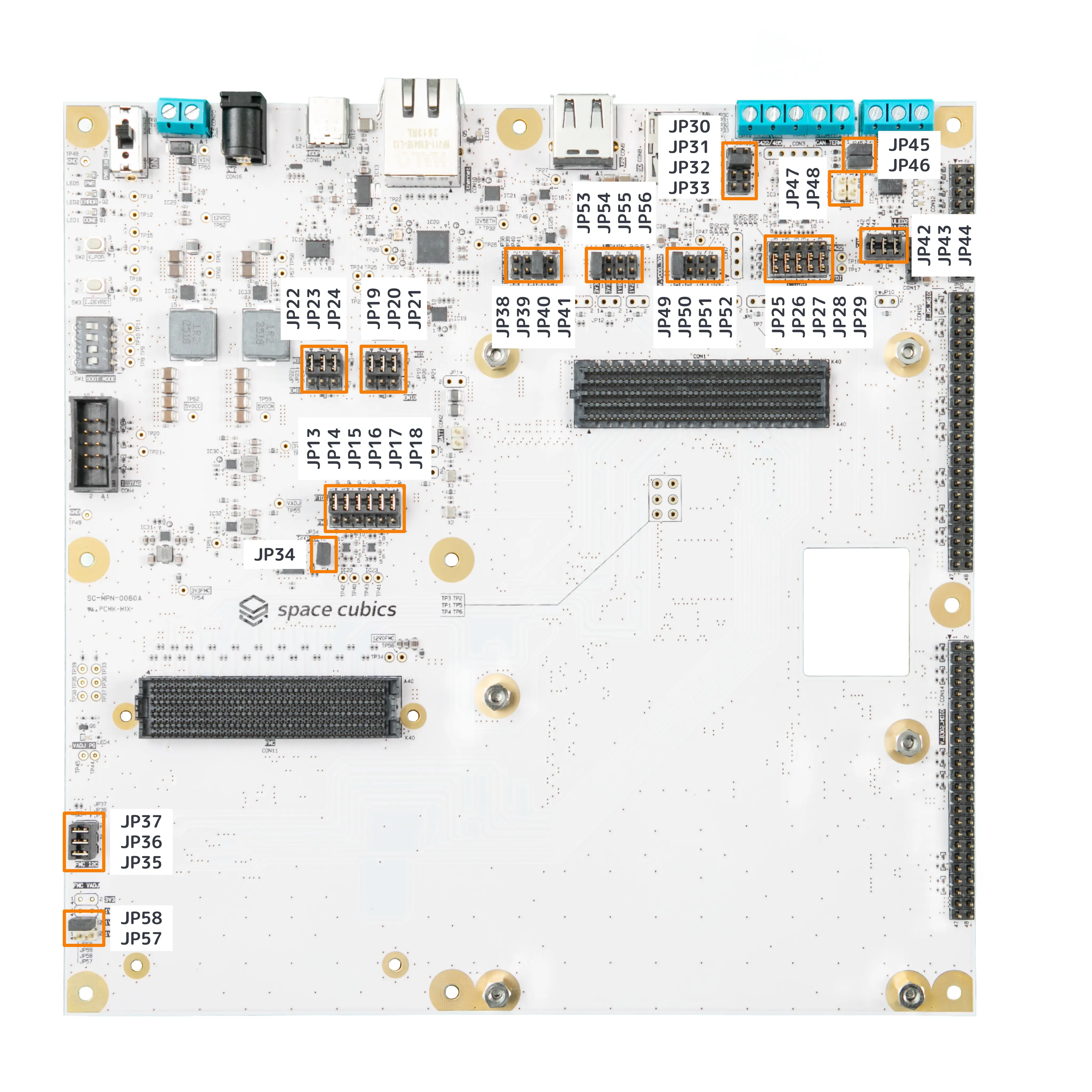
| Part Number | Interface Name | Form Factor |
|---|---|---|
JP13-JP18 |
Versal FPGA JTAG Selector |
Pin header 18 pins (6 pins x 3 rows / 2.54mm pitch) |
JP19-JP21 |
Versal APU/RPU Console (UART0) Selector |
Pin header 9 pins (3 pins x 3 rows / 2.54mm pitch) |
JP22-JP24 |
Versal APU/RPU Console (UART1) Selector |
Pin header 9 pins (3 pins x 3 rows / 2.54mm pitch) |
JP25-JP29 |
IGLOO2 Telemetry/Telecommand Selector |
Pin header 15 pins (5 pins x 3 rows / 2.54mm pitch) |
JP30-JP33 |
RS-422/RS-485 Communication Setting Selector |
Pin header 8 pins (4 pins x 2 rows / 2.54mm pitch) |
JP34 |
Versal GTYP Selector |
Pin header 2 pins (2.54mm pitch) |
JP35-JP37 |
Versal I2C Selector |
Pin header 6 pins (3 pins x 2 rows / 2.54mm pitch) |
JP38-JP41 |
Versal Bank 502 Power Selector |
Pin header 8 pins (4 pins x 2 rows / 2.54mm pitch) |
JP42-JP44 |
Versal CAN Selector |
Pin header 6 pins (3 pins x 2 rows / 2.54mm pitch) |
JP45-JP46 |
Versal CAN Termination Selector |
Pin header 4 pins (2 pins x 2 rows / 2.54mm pitch) |
JP47-JP48 |
Versal MIO Communication Direction Selector |
Pin header 4 pins (2 pins x 2 rows / 2.54mm pitch) |
JP49-JP52 |
Versal Bank 302 Power Selector |
Pin header 8 pins (4 pins x 2 rows / 2.54mm pitch) |
JP53-JP56 |
IGLOO2 Bank 5 Power Selector |
Pin header 8 pins (4 pins x 2 rows / 2.54mm pitch) |
JP57-JP58 |
FMC Module I/O Voltage Selector |
Pin header 4 pins (2 pins x 2 rows / 2.54mm pitch) |
Versal JTAG Selector (JP13-JP18)
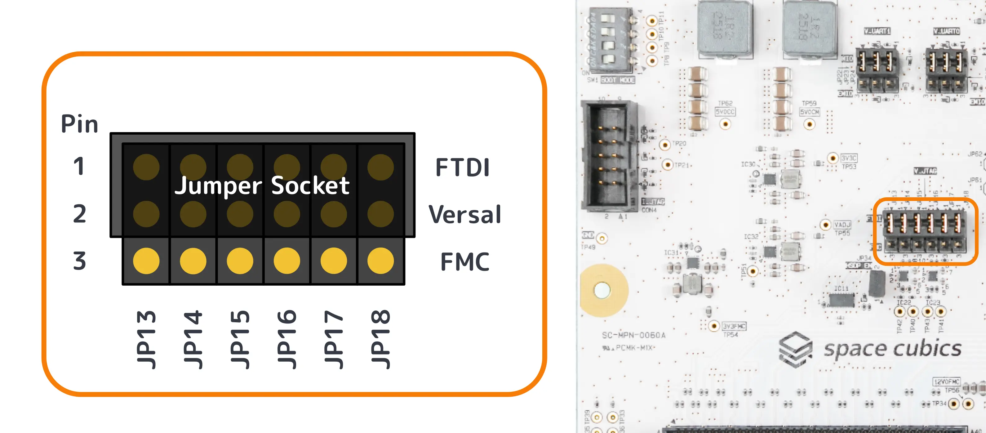
JP13-JP18 are interfaces capable of switching the connection destination of the Versal FPGA JTAG interface.
When jumper sockets are inserted between Pin.1-2, it connects to Channel A of the FTDI IC, enabling access from CON6 (USB Type-C).
By inserting them between Pin.2-3, it becomes possible to communicate with the FMC module connected to CON11 via level shifters (IC22, IC23).
|
Jumper sockets are inserted between Pin.1-2 by default, and since it is a 2 x 6 size, 6 pins can be switched at a time. |
REF |
Pin Number |
I/O |
||
1 |
2 |
3 |
||
JP13 |
FTDI_JTAG_TMS |
XCVE_JTAG_TMS |
FMC_JTAG_TMS |
Input |
JP14 |
FTDI_JTAG_TDI |
XCVE_JTAG_TDI |
FMC_JTAG_TDI |
Input |
JP15 |
FTDI_JTAG_TDO |
XCVE_JTAG_TDO |
FMC_JTAG_TDO |
Output |
JP16 |
FTDI_JTAG_TCK |
XCVE_JTAG_TCK |
FMC_JTAG_TCK |
Input |
JP17 |
GND |
GND |
GND |
Power |
JP18 |
VDD_FTDI_JTAG |
VDD_1V8_B503 |
VDD_FMC_JTAG |
Power |
Versal APU/RPU Console (UART0) Selector (JP19-JP21)
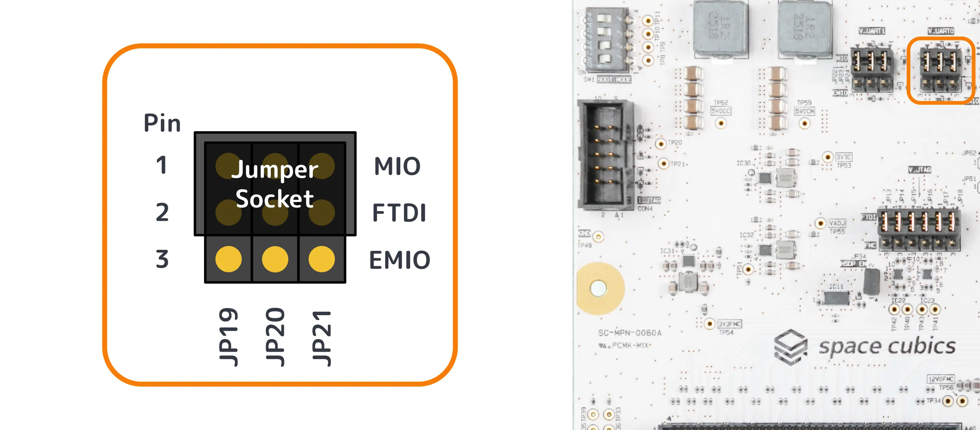
JP19-JP21 are interfaces capable of switching the connection destination to Channel B of the FTDI IC.
When jumper sockets are inserted between Pin.1-2, it connects to UART0 mapped to the Versal LPD MIO.
By inserting them between Pin.2-3, it connects to UART0 (EMIO) mapped to the Versal HDIO.
After connection, access is possible from CON6 (USB Type-C).
|
Jumper sockets are inserted between Pin.1-2 by default, and since it is a 2 x 3 size, 3 pins can be switched at a time. |
| Pin Name | Pin Number | ||
|---|---|---|---|
REF |
1 |
2 |
3 |
JP19 |
VDD_B502 |
VDD_FTDI_BDBUS |
VDD_B302 |
JP20 |
LPD_MIO0_UART0_RXD |
FTDI_BDBUS_TXD |
HDIO_302_L8P_UART0_RXD |
JP21 |
LPD_MIO1_UART0_TXD |
FTDI_BDBUS_RXD |
HDIO_302_L8N_UART0_TXD |
|
VDD: Power / RXD: Input / TXD: Output |
Versal APU/RPU Console (UART1) Selector (JP22-JP24)
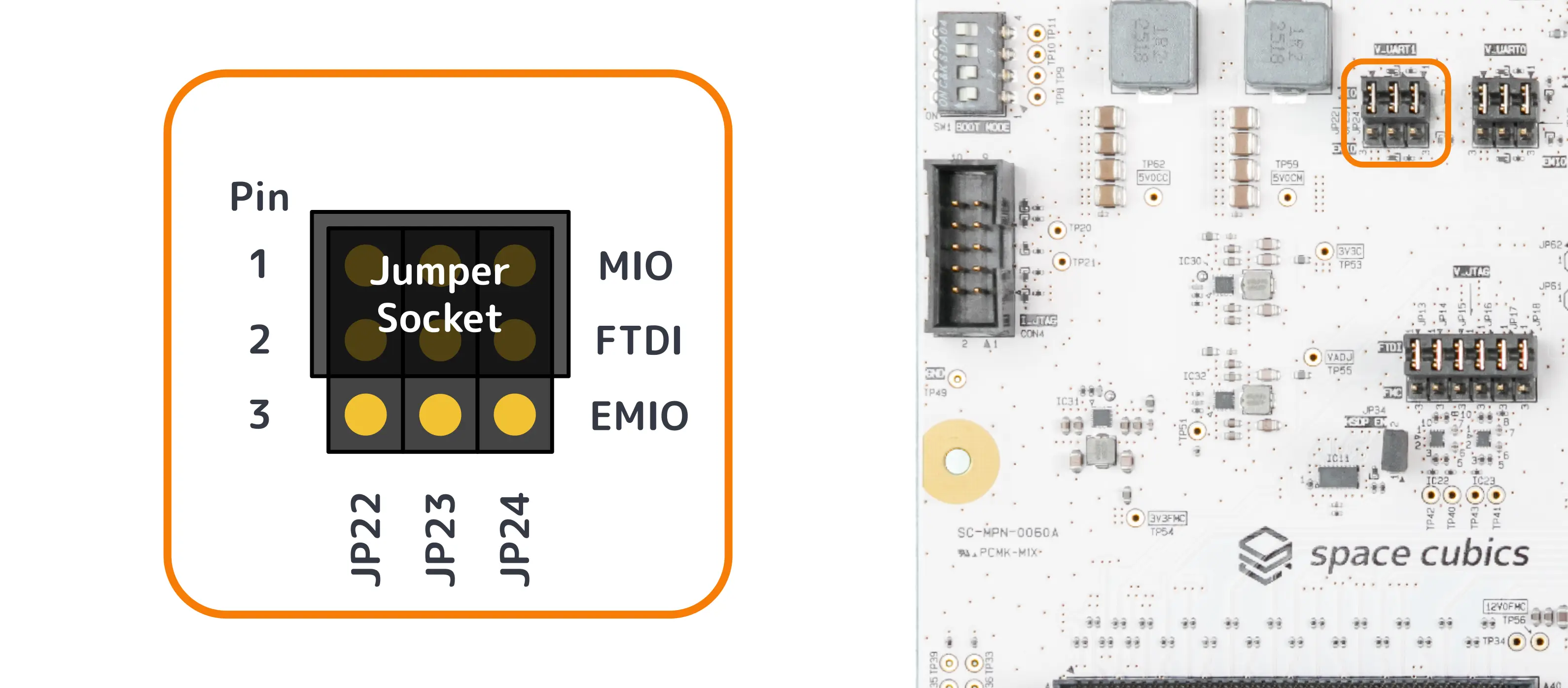
JP22-JP24 are interfaces capable of switching the connection destination to Channel C of the FTDI IC.
When jumper sockets are inserted between Pin.1-2, it connects to UART1 mapped to the Versal LPD MIO.
By inserting them between Pin.2-3, it connects to UART1 (EMIO) mapped to the Versal HDIO.
After connection, access is possible from CON6 (USB Type-C) for both.
|
Jumper sockets are inserted between Pin.1-2 by default, and since it is a 2 x 3 size, 3 pins can be switched at a time. |
| Pin Name | Pin Number | ||
|---|---|---|---|
REF |
1 |
2 |
3 |
JP19 |
VDD_B502 |
VDD_FTDI_CDBUS |
VDD_B302 |
JP20 |
LPD_MIO5_UART1_RXD |
FTDI_CDBUS_TXD |
HDIO_302_L10P_UART1_RXD |
JP21 |
LPD_MIO4_UART1_TXD |
FTDI_CDBUS_RXD |
HDIO_302_L10N_UART1_TXD |
|
VDD: Power / RXD: Input / TXD: Output |
IGLOO2 Telemetry/Telecommand Selector (JP25-JP29)
JP25-JP29 are interfaces capable of switching the connection destination of the IGLOO2 UART.
By accessing the IGLOO2 UART, it is possible to monitor via Telemetry signals from the OBC or change modes via Telecommand signals to the OBC.
When jumper sockets are inserted between Pin.1-2, it connects to Channel D of the FTDI IC, enabling access from CON6 (USB Type-C).
By inserting them between Pin.2-3, access becomes possible from CON18 using devices compatible with the RS-422/RS-485 standard.
|
Jumper sockets are inserted between Pin.1-2 by default, and since it is a 2 x 5 size, 5 pins can be switched at a time. |
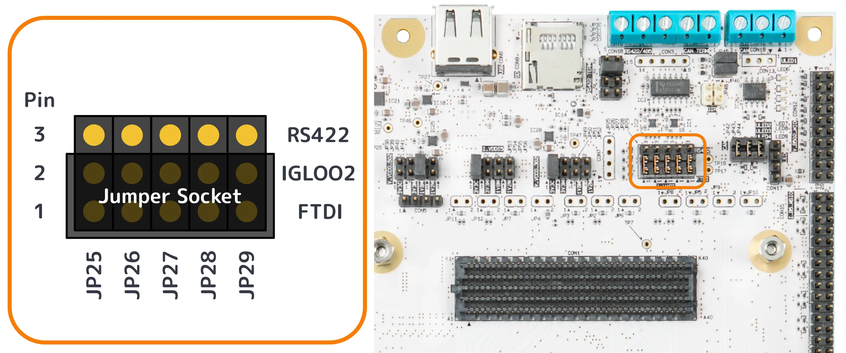
| Pin Name | Pin Number | ||
|---|---|---|---|
REF |
1 |
2 |
3 |
JP25 |
VDD_FTDI_DDBUS |
VDD_1V8_M |
VDD_RS422 |
JP26 |
FTDI_DDBUS_TXD |
M2GL_UART_RX |
RS422_R |
JP27 |
FTDI_DDBUS_RXD |
M2GL_UART_TX |
RS422_D |
JP28 |
NC |
M2GL_UART_DE |
RS422_DE |
JP29 |
NC |
M2GL_UART_RE_B |
RS422_RE_B |
|
VDD: Power / RXD,RX,D: Input / TXD,TX,R: Output |
RS-422/RS-485 Communication Setting Selector (JP30-JP33)
JP30-JP33 are interfaces to configure when connecting RS-422/RS-485 compatible devices to CON18 to communicate with the OBC.
Please set the jumper sockets according to the corresponding device by referring to the table below.
|
By default, a jumper socket is inserted in JP31. |
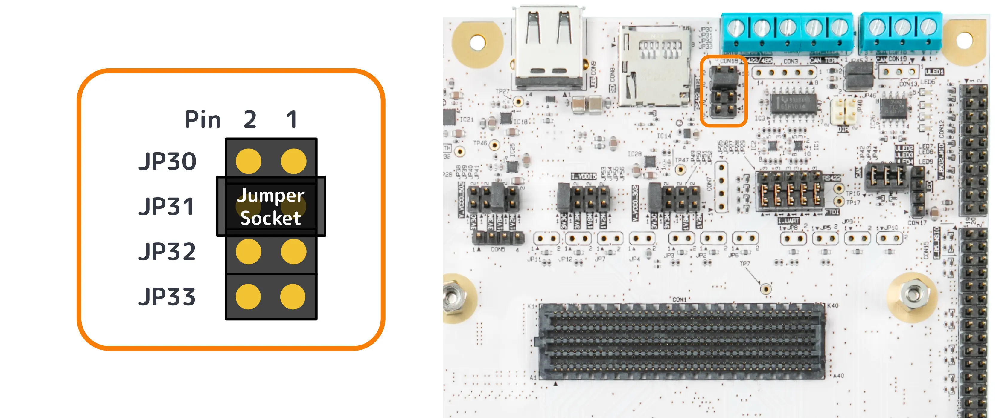
| REF | Description |
|---|---|
JP30 |
Interface to select the presence of a Driver termination resistor. |
JP31 |
Interface to select the presence of a Receiver termination resistor. |
JP32 |
Interface capable of short-circuiting the Y and A terminals of the Transceiver. |
JP33 |
Interface capable of short-circuiting the Z and B terminals of the Transceiver. |
|
When terminating in half-duplex communication, please insert a jumper socket into either JP30 or JP31. |
Versal GTYP Selector (JP34)
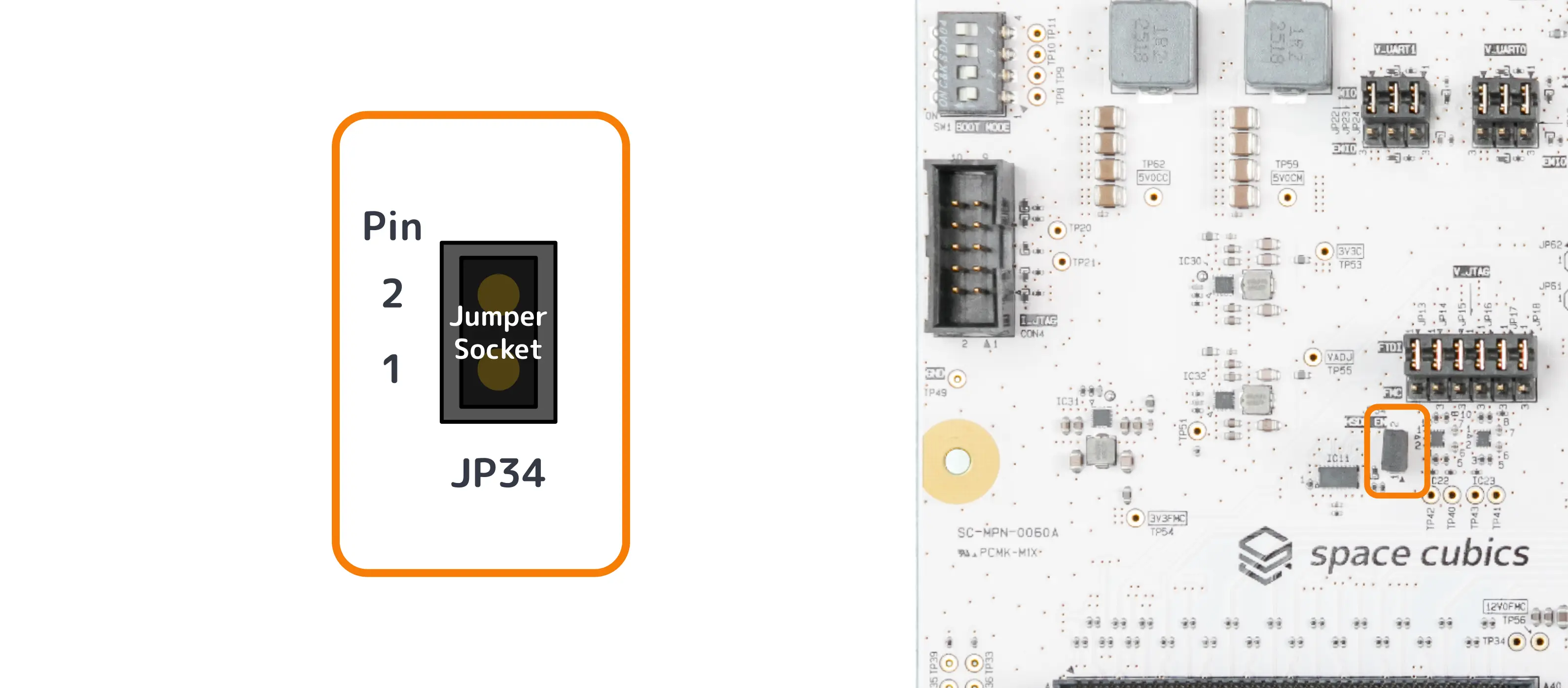
JP34 is an interface capable of switching the connection destination of GTYP, which is Versal’s high-speed serial communication signal.
Please insert a jumper socket if you wish to perform high-speed debugging and tracing of Versal using a SmartLynq+ module utilizing CON6 (USB Type-C).
If you do not perform the above and wish to evaluate the target GTYP with the FMC module connected to CON11, do not insert a jumper socket.
Versal I2C Selector (JP35-JP37)
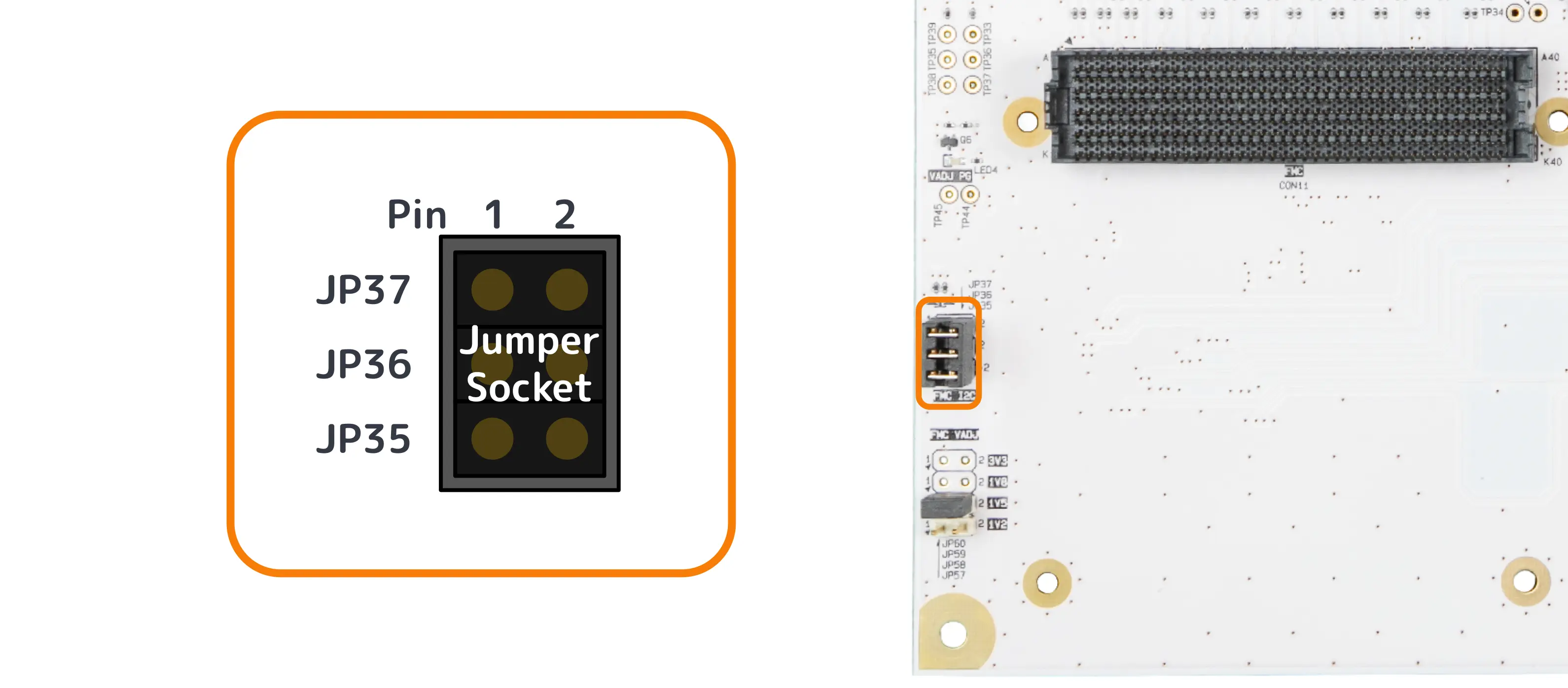
JP35-JP37 are interfaces used when you want to utilize the Versal LPD MIO mapped to I2C0 with the FMC module.
Please insert jumper sockets if you want to use it with the FMC module.
The Versal LPD MIO will be connected to the FMC module connected to CON11 via a level shifter (IC24).
|
By default, 2 x 3 size jumper sockets are inserted into JP35-JP37. |
|
The target Versal LPD MIO is also routed to CON12. |
Versal Bank 502 Power Selector (JP38-JP41)
JP38-JP41 are interfaces capable of switching the power domain of the Versal LPD MIO.
Please refer to the table below for power assignments.
The voltage selected here is also supplied to CON12.
|
By default, the power for JP40 is selected. |
|
When using CON10 (Ethernet) or CON19 (CAN), please select a voltage of 1.8V or higher. |
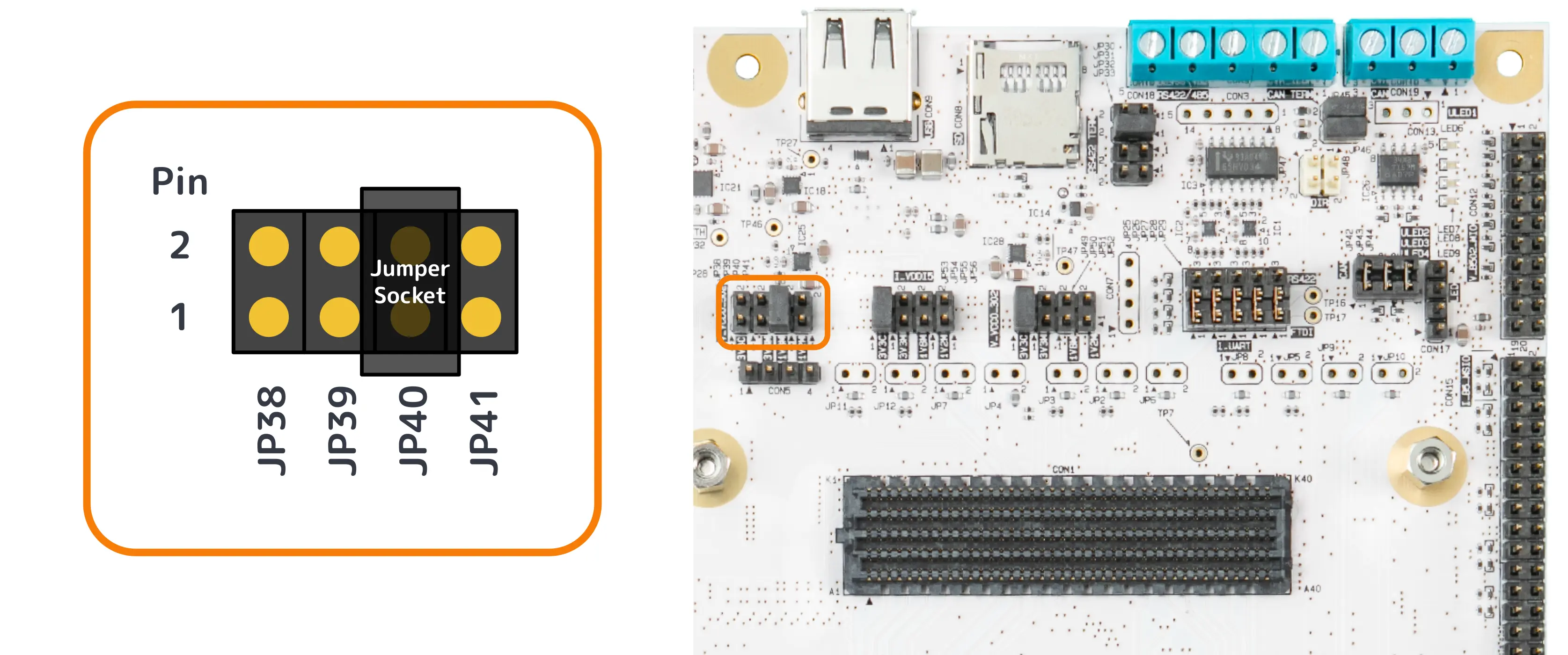
| REF | Pin Name | Description |
|---|---|---|
JP38 |
VDD_3V3_C |
+3.3V power generated from the Dev Board main power |
JP39 |
VDD_3V3_M |
+3.3V power generated by the OBC |
JP40 |
VDD_1V8_M |
+1.8V power generated by the OBC. Has a current limit of approx. 0.5A. |
JP41 |
VDD_1V2_M |
+1.2V power generated by the OBC. Has a current limit of approx. 0.5A. |
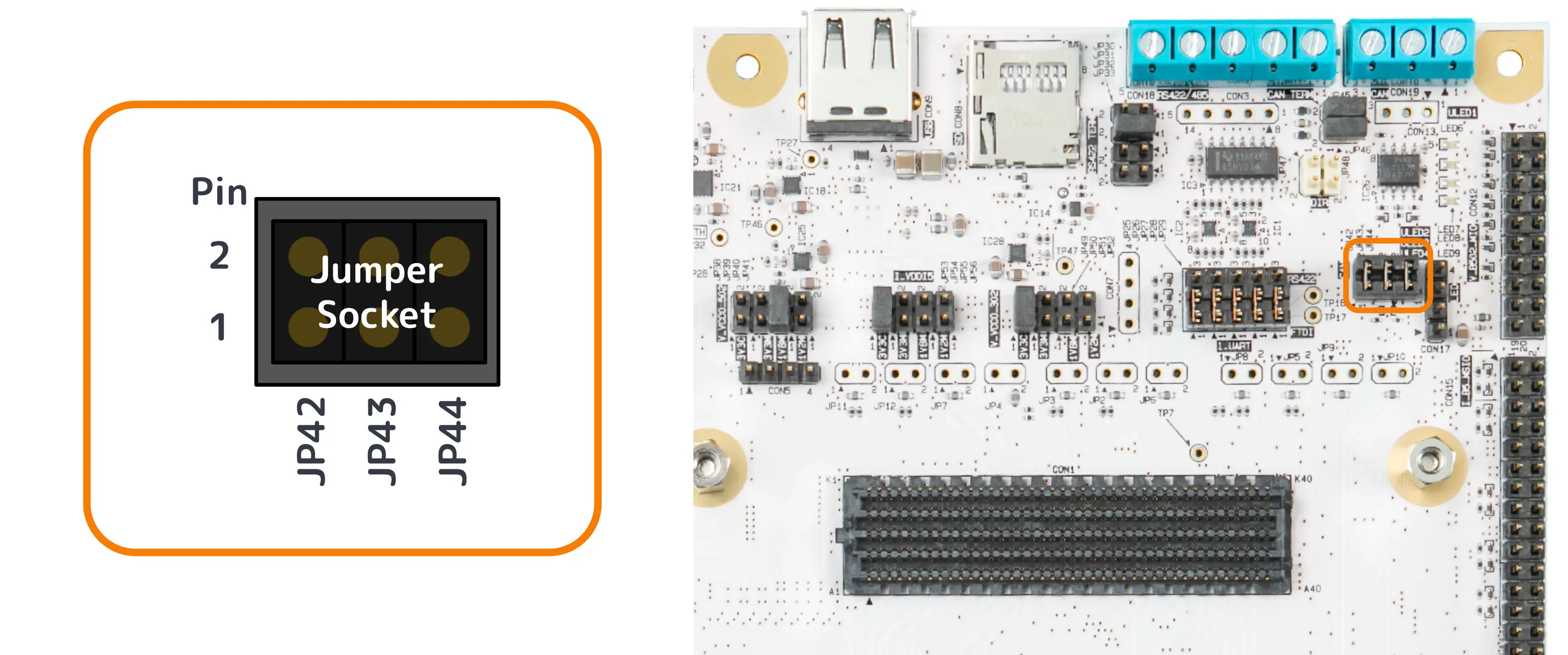
Versal CAN Selector (JP42-JP44)
JP42-JP44 are interfaces used when you wish to perform CAN communication with Versal utilizing CON19.
Please insert jumper sockets if you want to connect a CAN compatible device to CON19 to communicate with Versal.
|
By default, 2 x 3 size jumper sockets are inserted into JP42-JP44. |
|
The target Versal LPD MIO is also routed to CON12. |
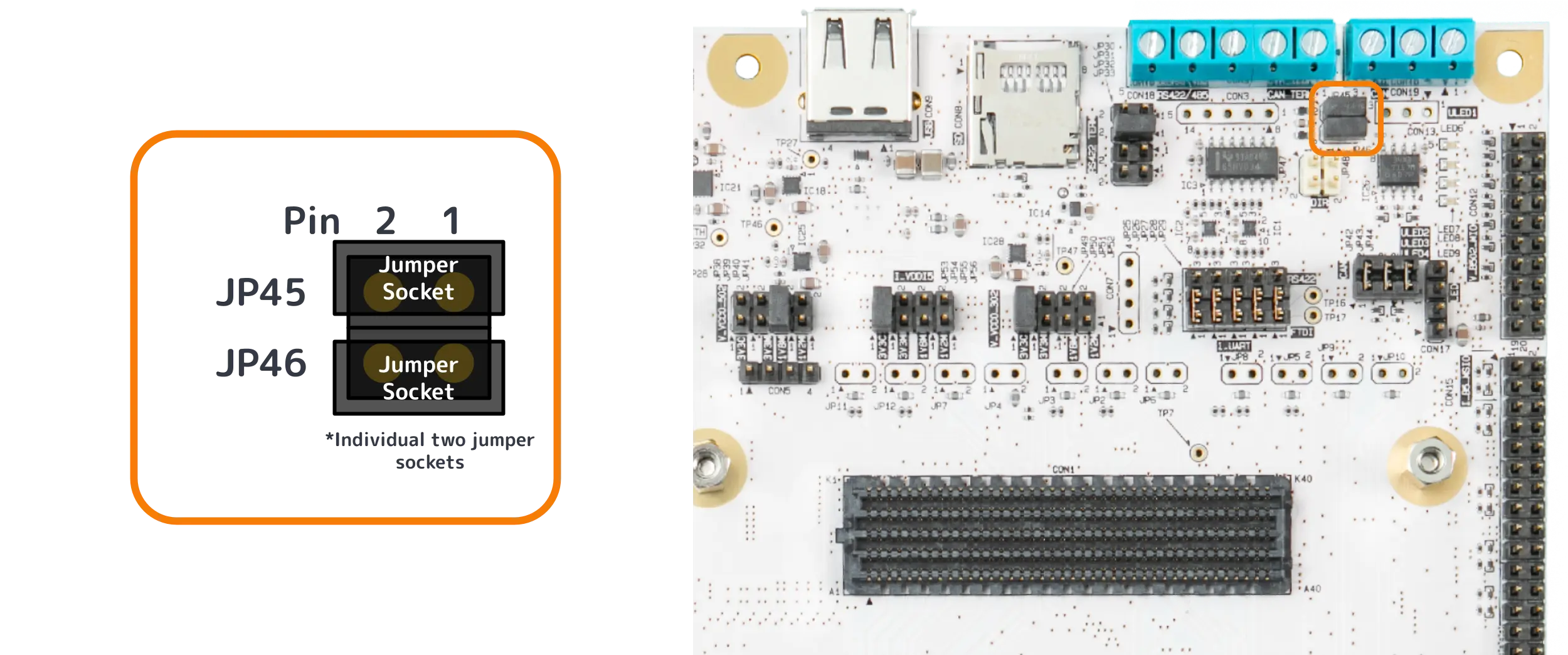
Versal CAN Termination Selector (JP45-JP46)
JP45-JP46 are interfaces to select the presence of a CAN termination resistor.
Please insert jumper sockets if a CAN termination resistor is required.
|
By default, two 1 x 2 size jumper sockets are inserted. |
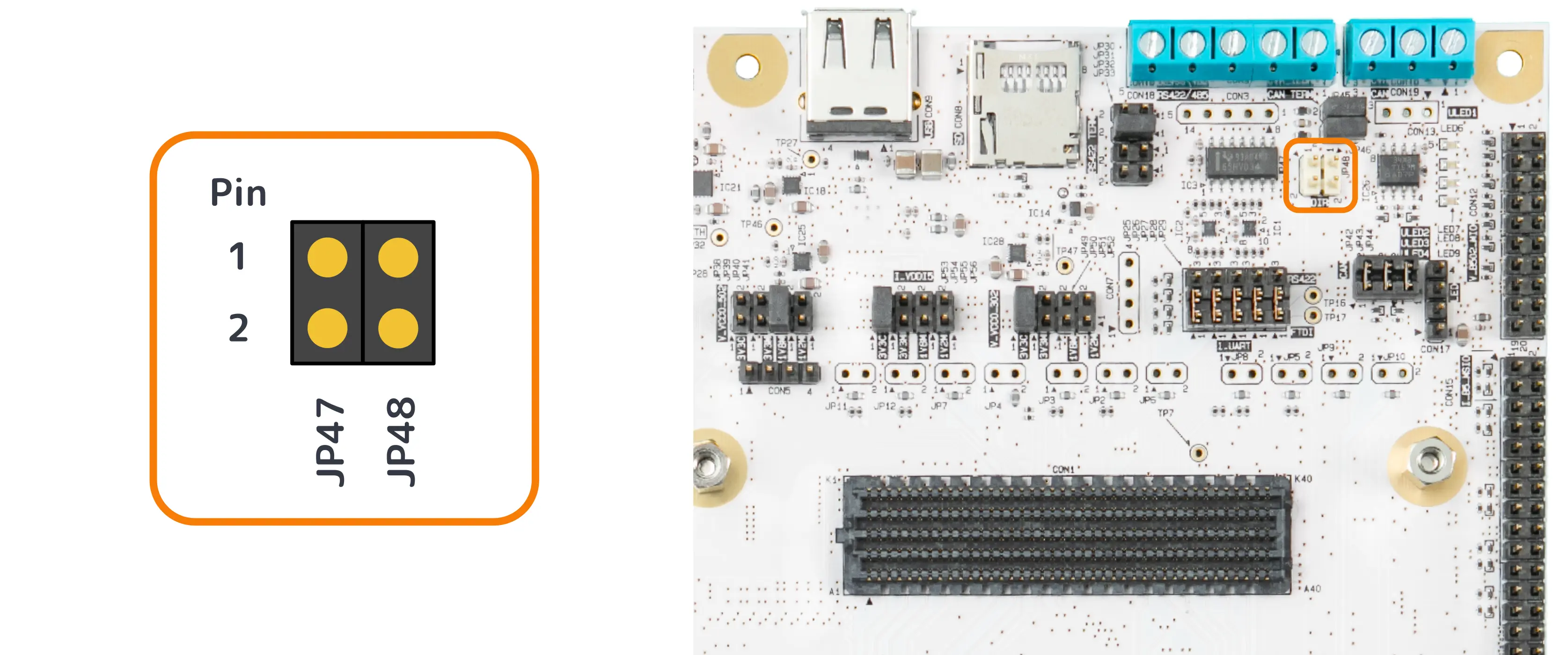
Versal MIO Communication Direction Selector (JP47-JP48)
JP47-JP48 are interfaces configured according to the communication direction of Versal PMC MIO 0 and Versal PMC MIO 1 connected to CON12.
Because the target MIO passes through a level shifter (IC27) on its way to CON12, it is necessary to set the communication direction of the level shifter according to the MIO’s communication direction.
The table below shows the input/output directions as seen from CON12 when a jumper socket is inserted or removed.
|
By default, no jumper sockets are inserted. |
| REF | Target MIO | Jumper Socket | CON12 Pin Direction |
|---|---|---|---|
JP47 |
PMC_MIO12_3V3 |
Inserted |
Output |
Removed |
Input |
||
JP48 |
PMC_MIO37_3V3 |
Inserted |
Output |
Removed |
Input |
Versal Bank 302 Power Selector (JP49-JP52)
JP49-JP52 are interfaces capable of switching the power domain of the Versal HDIO.
Please refer to the table below for power assignments.
The voltage selected here is also supplied to CON14.
|
By default, the power for JP49 is selected. |
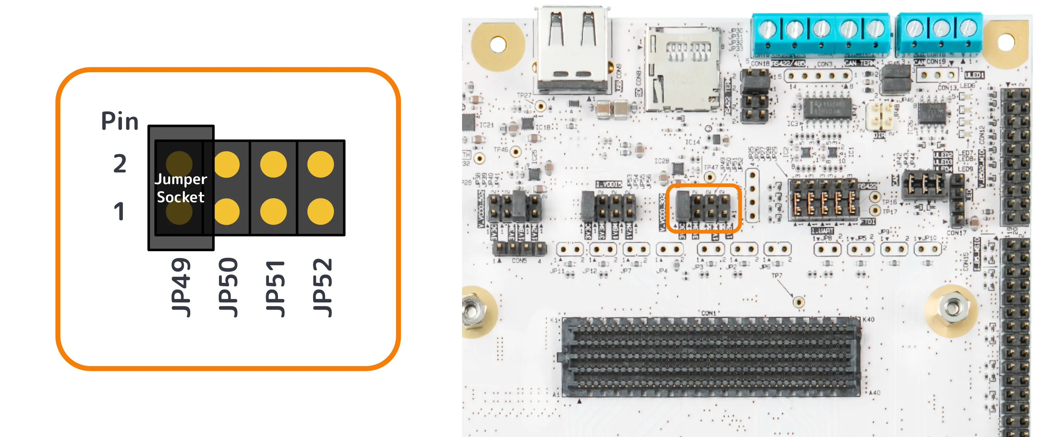
| REF | Pin Name | Description |
|---|---|---|
JP49 |
VDD_3V3_C |
+3.3V power generated from the Dev Board main power |
JP50 |
VDD_3V3_M |
+3.3V power generated by the OBC |
JP51 |
VDD_1V8_M |
+1.8V power generated by the OBC. Has a current limit of approx. 0.5A. |
JP52 |
VDD_1V2_M |
+1.2V power generated by the OBC. Has a current limit of approx. 0.5A. |
IGLOO2 Bank 5 Power Selector (JP53-JP56)
JP53-JP56 are interfaces capable of switching the power domain of the IGLOO2 MSIO (Bank 5).
Please refer to the table below for power assignments.
The voltage selected here is also supplied to CON15.
|
By default, the power for JP53 is selected. |
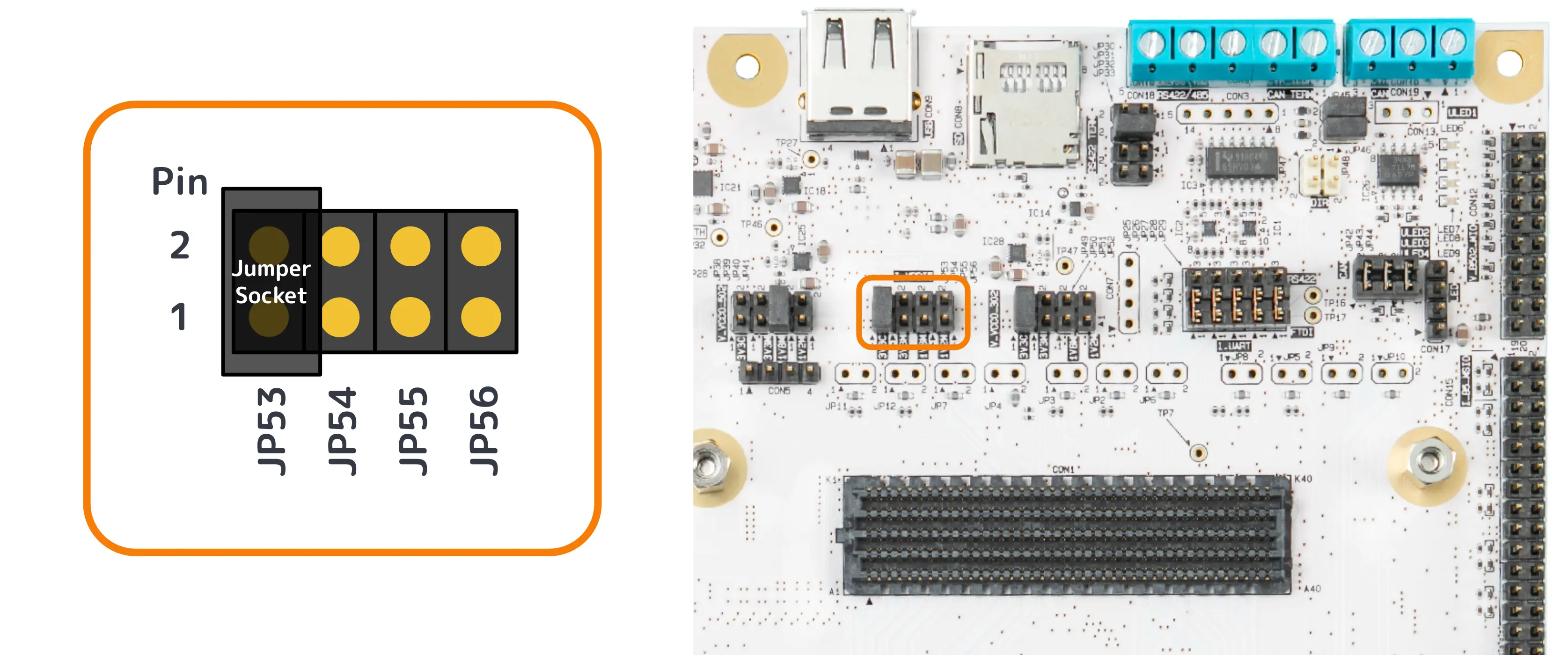
| REF | Pin Name | Description |
|---|---|---|
JP53 |
VDD_3V3_C |
+3.3V power generated from the Dev Board main power |
JP54 |
VDD_3V3_M |
+3.3V power generated by the OBC |
JP55 |
VDD_1V8_M |
+1.8V power generated by the OBC. Has a current limit of approx. 0.5A. |
JP56 |
VDD_1V2_M |
+1.2V power generated by the OBC. Has a current limit of approx. 0.5A. |
FMC Module I/O Voltage Selector (JP57-JP58)
JP57-JP58 are interfaces that allow selecting the power domain of the Versal XPIO and IGLOO2 MSIO (Bank 8) connected to the FMC module.
Since it is similarly supplied to the VADJ terminal of CON11, communication becomes possible at the selected power domain here.
|
By default, a jumper socket is inserted into JP58. |
|
Inserting jumper sockets into both JP57 and JP58 will result in an unintended voltage. |
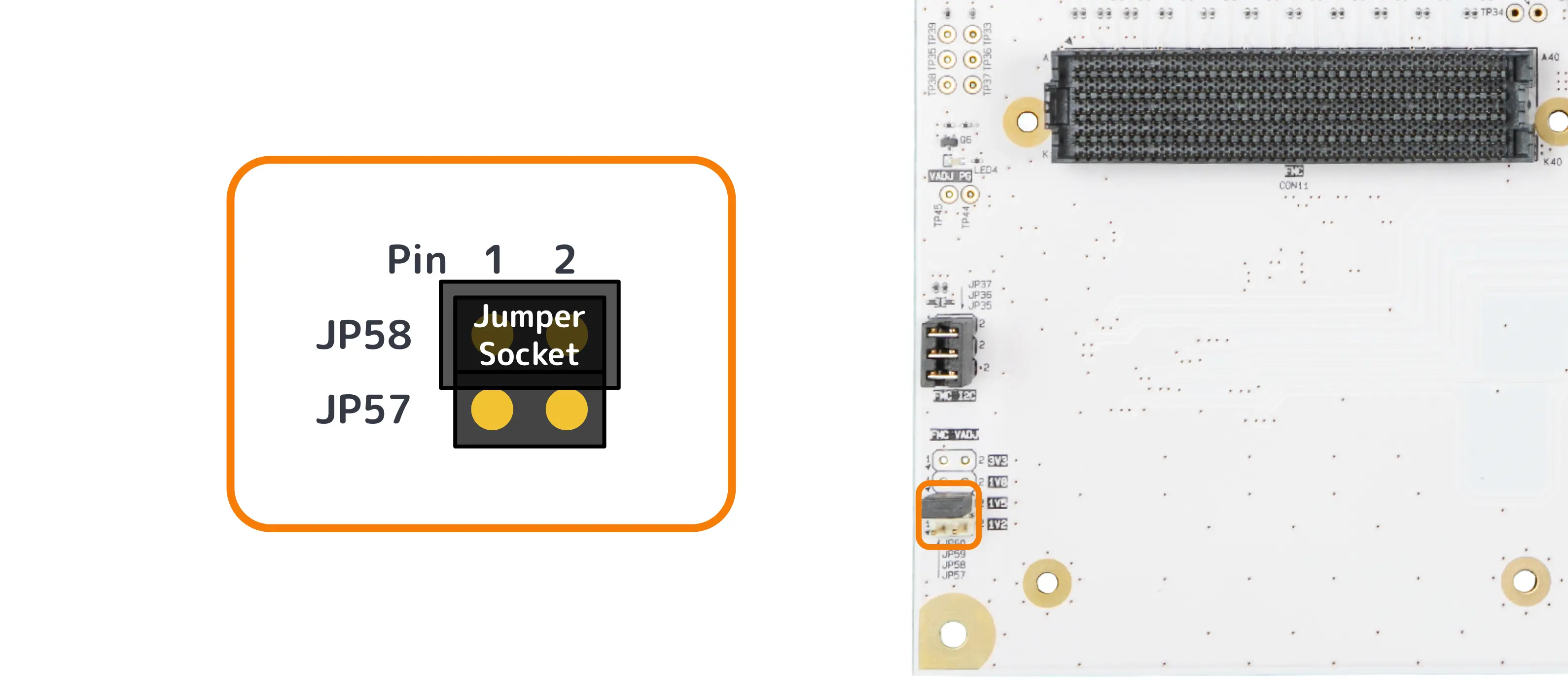
| REF | Power Domain |
|---|---|
JP57 |
1.2V |
JP58 |
1.5V |