Connectors (CON)
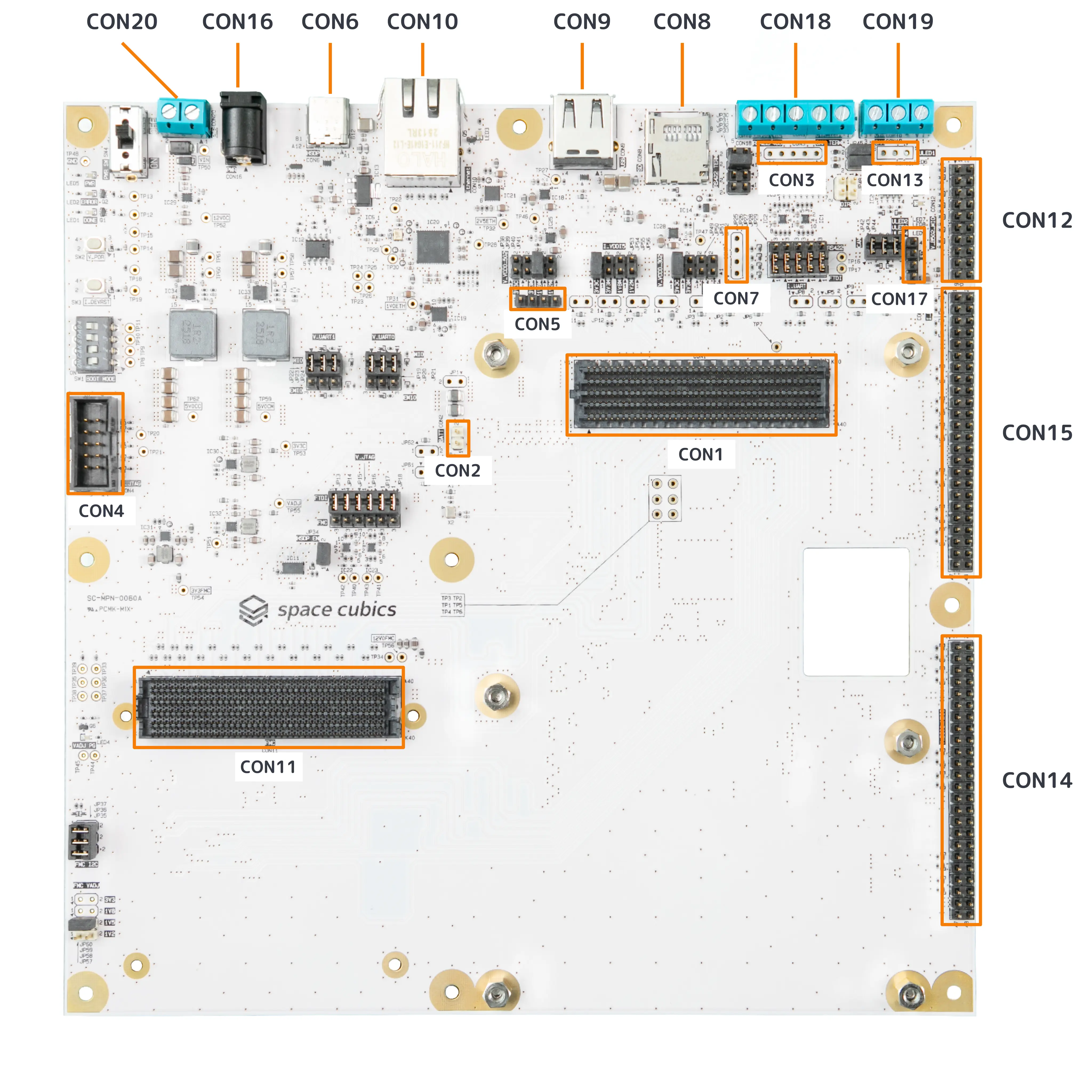
| Part Number | Interface Name | Form Factor | Remarks |
|---|---|---|---|
CON1 |
OBC Interface |
Board-to-board connector 400 pins (Terminal type / 1.27mm pitch) |
Mating cycles: 1,000 times |
CON2 |
BPD Power Supply Interface |
Pin header 2 pins (2.54mm pitch) |
|
CON3 |
CON18 Signal Observation Interface |
Pin header 5 pins (2.54mm pitch) |
Connector not installed |
CON4 |
IGLOO2 FPGA JTAG Interface |
Shrouded pin header 10 pins (5 pins x 2 rows / 2.54mm pitch) |
|
CON5 |
IGLOO2 Debug Interface |
Pin header 4 pins (2.54mm pitch) |
|
CON6 |
Versal / IGLOO2 Debug Interface |
USB Type.C Connector |
|
CON7 |
Versal Reserve Interface |
Pin header 4 pins (2.54mm pitch) |
Connector not installed |
CON8 |
microSD Card Interface |
microSD Connector |
|
CON9 |
USB2.0 Interface |
USB Type.A Connector |
|
CON10 |
Gigabit Ethernet Interface |
Gigabit Ethernet Connector |
|
CON11 |
Interface for FMC Module Connection |
Board-to-board connector 400 pins (Socket type / 1.27mm pitch) |
|
CON12 |
Versal MIO Expansion Interface |
Pin header 20 pins (10 pins x 2 rows / 2.54mm pitch) |
|
CON13 |
CON19 Signal Observation Interface |
Pin header 3 pins (2.54mm pitch) |
Connector not installed |
CON14 |
Versal HDIO Expansion Interface |
Pin header 48 pins (24 pins x 2 rows / 2.54mm pitch) |
|
CON15 |
IGLOO2 MSIO (Bank 5) Expansion Interface |
Pin header 48 pins (24 pins x 2 rows / 2.54mm pitch) |
|
CON16 |
Dev Board Main Power Supply Interface |
DC Jack |
Supported plug: 2.1mmΦ (Center positive) |
CON17 |
USER LED Control Interface |
Pin header 4 pins (2.54mm pitch) |
|
CON18 |
IGLOO2 RS422/485 Interface |
Terminal block 5 pins (5.0mm pitch) |
|
CON19 |
CAN Interface |
Terminal block 3 pins (5.0mm pitch) |
|
CON20 |
Dev Board Main Power Supply Interface |
Terminal block 2 pins (5.0mm pitch) |
OBC Interface (CON1)
CON1 is the connection interface with the OBC.
Installed connector: SEAM-40-02.0-S-10-1-A-K-TR (Samtec)
BPD Power Supply Interface (CON2)
CON2 is an interface capable of supplying power to the Versal’s Battery Power Domain (BPD).
The BPD encompasses the Real Time Clock (RTC) and Battery Backup RAM (BBRAM).
The RTC and BBRAM typically operate on the voltage (VCCAUX_PMC_SMON) generated within the OBC, but if the main power of the OBC is disconnected, they are maintained or retained by the voltage supplied from CON2.
| Pin Number | Pin Name | I/O | Power Domain | Description |
|---|---|---|---|---|
1 |
VCC_BATT_IN |
Power |
VCC_BATT_IN |
Power supply (VCC_BATT_IN) |
2 |
GND |
Power |
VCC_BATT_IN |
Ground |
CON18 Signal Observation Interface (CON3)
CON3 is an interface for observing communication signals with the device connected to CON18 using a probe.
The pin assignment of CON3 is identical to that of CON18, as shown in the table below.
For details on the signal lines, refer to the CON18 specifications.
| CON3 Pin Number |
Pin Name | CON18 Pin Number |
|---|---|---|
1 |
RS422_TXP |
1 |
2 |
RS422_TXM |
2 |
3 |
RS422_RXP |
3 |
4 |
RS422_RXM |
4 |
5 |
GND |
5 |
IGLOO2 FPGA JTAG Interface (CON4)
CON4 is the FPGA JTAG interface for the IGLOO2.
The pinout is compatible with Microchip’s FPGA debugger, FlashPro5.
-
Odd pin row
| Pin Number | Pin Name | I/O | Power Domain | Description |
|---|---|---|---|---|
1 |
M2GL_JTAG_TCK |
Input |
VDD_1V8_M2GL_B4 |
IGLOO2 JTAG Clock |
3 |
M2GL_JTAG_TDO |
Output |
VDD_1V8_M2GL_B4 |
IGLOO2 JTAG Data Output |
5 |
M2GL_JTAG_TMS |
Input |
VDD_1V8_M2GL_B4 |
IGLOO2 JTAG Selection |
7 |
NC |
- |
VDD_1V8_M2GL_B4 |
Connect to TP20 |
9 |
M2GL_JTAG_TDI |
Input |
VDD_1V8_M2GL_B4 |
IGLOO2 JTAG Data Output |
-
Even pin row
| Pin Number | Pin Name | I/O | Power Domain | Description |
|---|---|---|---|---|
2 |
GND |
Power |
VDD_1V8_M2GL_B4 |
Ground |
4 |
NC |
- |
VDD_1V8_M2GL_B4 |
Connect to TP21 |
6 |
VDD_1V8_M2GL_B4 |
Power |
VDD_1V8_M2GL_B4 |
Power supply (VDD_1V8_M2GL_B4) |
8 |
M2GL_JTAG_TRSTB |
Input |
VDD_1V8_M2GL_B4 |
IGLOO2 JTAG Reset |
10 |
GND |
Power |
VDD_1V8_M2GL_B4 |
Ground |
IGLOO2 Debug Interface (CON5)
Pins 2 and 3 of CON5 are assigned to the IGLOO2 UART and can be used as a console.
Pins 1 and 4 are IGLOO2 reserved pins.
| Pin Number | Pin Name | I/O | Power Domain | Description |
|---|---|---|---|---|
1 |
M2GL_RSVD0 |
In/Out |
VDD_1V8_M2GL_B4 |
Reserve |
2 |
M2GL_RSVD1 |
Output |
VDD_1V8_M2GL_B4 |
IGLOO2 UART TXD |
3 |
M2GL_RSVD2 |
Input |
VDD_1V8_M2GL_B4 |
IGLOO2 UART RXD |
4 |
M2GL_RSVD3 |
In/Out |
VDD_1V8_M2GL_B4 |
Reserve |
Versal / IGLOO2 Debug Interface (CON6)
CON6 is the debug interface for Versal and IGLOO2.
It is equipped with an FTDI IC, allowing the selection of the following debug methods:
-
Versal FPGA JTAG
-
Versal APU/RPU Console
-
IGLOO2 Safety Processor Telemetry/Telecommand
Additionally, the Versal high-speed serial communication signal GTYP is connected to CON6 via a bidirectional high-speed multiplexer, enabling debugging with the Versal SmartLynq+ HSDP.
Versal FPGA JTAG
This is the Versal FPGA JTAG interface.
When the jumper sockets inserted in JP13-JP18 are switched to the "FTDI" silkscreen side, it connects to Channel A of the FTDI IC and becomes available for use.
Versal APU/RPU Console
This is the console for the Versal APU/RPU.
By switching the jumper sockets inserted in JP19-JP24, the serial communication signals mapped to the Versal UART are connected to the FTDI IC and become available for use.
Versal UART0 is connected to Channel B of the FTDI IC, and UART1 is connected to Channel C.
There are two types of serial communication signals: Versal LPD MIO and Versal HDIO. Since they are independent, even if one serial communication signal is used in a test, the other can be used as a console.
| FTDI IC Channel | Mapping | I/O | Select JP |
|---|---|---|---|
B |
UART0 |
Versal LPD MIO |
JP19~JP21: 1-2 |
Versal HDIO |
JP19~JP21: 2-3 |
||
C |
UART1 |
Versal LPD MIO |
JP22~JP24: 1-2 |
Versal HDIO |
JP22~JP24: 2-3 |
IGLOO2 Safety Processor Telemetry/Telecommand
Using the IGLOO2 UART, it is possible to monitor via Telemetry signals from the OBC or change modes via Telecommand signals to the OBC.
When the jumper sockets inserted in JP25-JP29 are switched to the "FTDI" silkscreen side, it connects to Channel D of the FTDI IC and becomes available for use.
Versal Reserve Interface (CON7)
Versal PMC MIO 1 is connected to CON7.
The MIO connected to CON7 is used to control the communication direction when a level shifter is provided between it and the microSD card interface.
Since the Dev Board uses a level shifter capable of bidirectional communication, this function is unnecessary, hence it is designated as Reserve.
| Pin Number | Pin Name | I/O | Power Domain | Description |
|---|---|---|---|---|
1 |
PMC_MIO46_SD0_DIRC |
Output |
VDD_1V8_PMC |
Connected to Versal(PMC_501_MIO46) |
2 |
PMC_MIO47_SD0_DIR0 |
Output |
VDD_1V8_PMC |
Connected to Versal(PMC_501_MIO47) |
3 |
PMC_MIO48_SD0_DIR1 |
Output |
VDD_1V8_PMC |
Connected to Versal(PMC_501_MIO48) |
4 |
NC |
- |
- |
- |
microSD Card Interface (CON8)
CON8 is an interface where a microSD card can be inserted.
In the early stages of development, it is assumed that the software for booting will be written to and used from a microSD card instead of the Flash memory or eMMC on the OBC.
USB2.0 Interface (CON9)
CON9 is an interface that allows the OBC to be used as a USB 2.0 host.
The VBUS, which is the power supplied from CON9, uses +5V generated from the main power of the Dev Board and routed through a load switch.
VBUS complies with USB 2.0.
Gigabit Ethernet Interface (CON10)
CON10 is a Gigabit Ethernet interface with an RJ45 type jack.
By porting the Linux OS to the Versal APU, remote login to the OBC becomes possible.
When the connection link is established, the green LED mounted on CON10 lights up.
During communication, the yellow LED also mounted on CON10 blinks.
When using CON10, select JP38-JP41 so that the power domain of the Versal LPD MIO is 1.8V or higher.
Interface for FMC Module Connection (CON11)
CON11 is an interface capable of connecting a commercially available FMC module for the purpose of evaluating the high-speed serial communication signals of Versal PL or IGLOO2.
The expected FMC modules for connection are as follows:
-
PCIe Gen3 x8 FMC Module by iWave (iW-FMC-PCIe-I2)
-
M.2 M-key Stack FMC by opsero (OP073)
-
RPi Camera FMC by opsero (OP068)
-
FMC XM105 Debug Card by AMD (HW-FMC-XM105-G)
Installed connector: ASP-134486-01 (Samtec)
Versal MIO Expansion Interface (CON12)
CON12 is an interface for bringing out the unused Versal MIO signals to the outside.
However, some LPD MIOs can be connected to circuits on the FTDI, CAN, or CON11 (Interface for FMC Module Connection) by jumper settings.
Please note that the Versal LPD MIO connected to Pins 1-8 of CON12 can be connected to circuits other than CON12 using jumper sockets.
The power supply (VDD_B502) connected to CON12 also serves as the power domain for the Versal LPD MIO, and its voltage can be selected with JP38-JP41.
In addition, a load switch is provided for VDD_B502, so that if the main power of Versal is disconnected, it will reliably disconnect the power to Versal Bank 502 as well.
Versal PMC MIO 0 and Versal PMC MIO 1, connected to Pins 13-14 of CON12, have a fixed power domain of 1.8V, so the power domain is converted to VDD_B502 via a level shifter (IC27) to match the Versal LPD MIO.
Therefore, please note that you must switch JP47-JP48 according to the communication direction of Pins 13-14.
| Pin Number | Pin Name | I/O | Power Domain | Description |
|---|---|---|---|---|
1 |
LPD_MIO0_UART0_RXD |
Input |
VDD_B502 |
Connected to CON1(J25) or JP20 (FTDI IC Channel.B) |
2 |
LPD_MIO1_UART0_TXD |
Output |
VDD_B502 |
Connected to CON1(K25) or JP21 (FTDI IC Channel.B) |
3 |
LPD_MIO2_CAN0_RX |
Input |
VDD_B502 |
Connected to CON1(J26) or JP44 (CAN Transceiver) |
4 |
LPD_MIO3_CAN0_TX |
Output |
VDD_B502 |
Connected to CON1(K26) or JP43 (CAN Transceiver) |
5 |
LPD_MIO4_UART1_TXD |
Output |
VDD_B502 |
Connected to CON1(J27) or JP24 (FTDI IC Channel.C) |
6 |
LPD_MIO5_UART1_RXD |
Input |
VDD_B502 |
Connected to CON1(K27) or JP23 (FTDI IC Channel.C) |
7 |
LPD_MIO6_I2C0_SCL |
Output |
VDD_B502 |
Connected to CON1(J28) or JP36 (Level shifter to CON11) |
8 |
LPD_MIO7_I2C0_SDA |
In/Out |
VDD_B502 |
Connected to CON1(K28) or JP37 (Level shifter to CON11) |
9 |
LPD_MIO8 |
In/Out |
VDD_B502 |
Connected to CON1(J29) |
10 |
LPD_MIO9 |
In/Out |
VDD_B502 |
Connected to CON1(K29) |
11 |
LPD_MIO10 |
In/Out |
VDD_B502 |
Connected to CON1(J30) |
12 |
LPD_MIO11 |
In/Out |
VDD_B502 |
Connected to CON1(K30) |
13 |
PMC_MIO12_3V3 |
In/Out |
VDD_B502 |
Connected to CON1(J33) via IC27 |
14 |
PMC_MIO37_3V3 |
In/Out |
VDD_B502 |
Connected to CON1(H33) via IC27 |
15 |
GND |
Power |
VDD_B502 |
Ground |
16 |
GND |
Power |
VDD_B502 |
Ground |
17 |
VDD_B502 |
Power |
VDD_B502 |
Power supply (VDD_B502) |
18 |
VDD_B502 |
Power |
VDD_B502 |
Power supply (VDD_B502) |
19 |
VDD_B502 |
Power |
VDD_B502 |
Power supply (VDD_B502) |
20 |
VDD_B502 |
Power |
VDD_B502 |
Power supply (VDD_B502) |
CON19 Signal Observation Interface (CON13)
CON13 is an interface for observing communication signals with the device connected to CON19 using a probe.
The pin assignment of CON13 is identical to that of CON19, as shown in the table below.
For details on the signal lines, refer to the CON19 specifications.
| CON13 Pin Number |
Pin Name | CON19 Pin Number |
|---|---|---|
1 |
CAN_CANL |
1 |
2 |
CAN_CANH |
2 |
3 |
GND |
3 |
Versal HDIO Expansion Interface (CON14)
CON14 is the interface where the Versal HDIO is connected.
It is divided into 3 blocks of 12 pins each, separated by NC pins, and the row of each block corresponds to the PMOD pinout.
When multiple PMODs are inserted into CON14, NC pins are placed in between so that the PMODs do not interfere with each other.
The power supply (VDD_B302) connected to CON14 also serves as the power domain for the Versal HDIO, and its voltage can be selected with JP49-JP52.
A load switch is provided for VDD_B302, so that if the main power of Versal is disconnected, it will reliably disconnect the power to Versal Bank 302 as well.
-
Block 1
| Pin Number | Pin Name | I/O | Power Domain | Description |
|---|---|---|---|---|
1 |
HDIO_302_L0P |
In/Out |
VDD_B302 |
Connected to CON1(A22) |
3 |
HDIO_302_L0N |
In/Out |
VDD_B302 |
Connected to CON1(B22) |
5 |
HDIO_302_L2P |
In/Out |
VDD_B302 |
Connected to CON1(A26) |
7 |
HDIO_302_L2N |
In/Out |
VDD_B302 |
Connected to CON1(B26) |
9 |
GND |
Power |
VDD_B302 |
Ground |
11 |
VDD_B302 |
Power |
VDD_B302 |
Power supply (VDD_B302) |
| Pin Number | Pin Name | I/O | Power Domain | Description |
|---|---|---|---|---|
2 |
HDIO_302_L1P |
In/Out |
VDD_B302 |
Connected to CON1(A24) |
4 |
HDIO_302_L1N |
In/Out |
VDD_B302 |
Connected to CON1(B22) |
6 |
HDIO_302_L3P |
In/Out |
VDD_B302 |
Connected to CON1(B23) |
8 |
HDIO_302_L3N |
In/Out |
VDD_B302 |
Connected to CON1(C23) |
10 |
GND |
Power |
VDD_B302 |
Ground |
12 |
VDD_B302 |
Power |
VDD_B302 |
Power supply (VDD_B302) |
-
Block 2
| Pin Number | Pin Name | I/O | Power Domain | Description |
|---|---|---|---|---|
19 |
HDIO_302_L4P |
In/Out |
VDD_B302 |
Connected to CON1(B25) |
21 |
HDIO_302_L4N |
In/Out |
VDD_B302 |
Connected to CON1(C25) |
23 |
HDIO_302_L6P_HDGC |
In/Out |
VDD_B302 |
Connected to CON1(D24) |
25 |
HDIO_302_L6N_HDGC |
In/Out |
VDD_B302 |
Connected to CON1(E24) |
27 |
GND |
Power |
VDD_B302 |
Ground |
29 |
VDD_B302 |
Power |
VDD_B302 |
Power supply (VDD_B302) |
| Pin Number | Pin Name | I/O | Power Domain | Description |
|---|---|---|---|---|
20 |
HDIO_302_L5P_HDGC |
In/Out |
VDD_B302 |
Connected to CON1(D22) |
22 |
HDIO_302_L5N_HDGC |
In/Out |
VDD_B302 |
Connected to CON1(E22) |
24 |
HDIO_302_L7P |
In/Out |
VDD_B302 |
Connected to CON1(D26) |
26 |
HDIO_302_L7N |
In/Out |
VDD_B302 |
Connected to CON1(E26) |
28 |
GND |
Power |
VDD_B302 |
Ground |
30 |
VDD_B302 |
Power |
VDD_B302 |
Power supply (VDD_B302) |
-
Block 3
| Pin Number | Pin Name | I/O | Power Domain | Description |
|---|---|---|---|---|
37 |
HDIO_302_L8P_UART0_RXD |
Input |
VDD_B302 |
Connected to CON1(E21) |
39 |
HDIO_302_L8N_UART0_TXD |
Output |
VDD_B302 |
Connected to CON1(F21) |
41 |
HDIO_302_L10P_UART1_RXD |
Input |
VDD_B302 |
Connected to CON1(E25) |
43 |
HDIO_302_L10N_UART1_TXD |
Output |
VDD_B302 |
Connected to CON1(F25) |
45 |
GND |
Power |
VDD_B302 |
Ground |
47 |
VDD_B302 |
Power |
VDD_B302 |
Power supply (VDD_B302) |
| Pin Number | Pin Name | I/O | Power Domain | Description |
|---|---|---|---|---|
38 |
HDIO_302_L9P |
In/Out |
VDD_B302 |
Connected to CON1(E23) |
40 |
HDIO_302_L9N |
In/Out |
VDD_B302 |
Connected to CON1(F23) |
42 |
NC |
- |
- |
- |
44 |
NC |
- |
- |
- |
46 |
GND |
Power |
VDD_B302 |
Ground |
48 |
VDD_B302 |
Power |
VDD_B302 |
Power supply (VDD_B302) |
| All pins not included in the table are NC. |
IGLOO2 MSIO (Bank 5) Expansion Interface (CON15)
CON15 is the interface where the IGLOO2 MSIO (Bank 5) is connected.
Like CON14, it is divided into 3 blocks of 12 pins each, and the row of each block corresponds to the PMOD pinout.
Similar to CON14, when multiple PMODs are inserted, the blocks are separated to prevent PMODs from interfering with each other. However, due to the large number of MSIOs, MSIOs are also connected between the blocks, which were NC pins in CON14.
CThe power supply (VDD_M2GL_B5) connected to CON15 also serves as the power domain for the IGLOO2 MSIO (Bank 5), and its voltage can be selected with JP53-JP56.
However, since the main power of IGLOO2 is linked to the main power of the Dev Board, unlike VDD_B502 and VDD_B302, no load switch is provided for VDD_M2GL_B5.
-
Block 1
| Pin Number | Pin Name | I/O | Power Domain | Description |
|---|---|---|---|---|
1 |
M2GL_MSIO196PB5 |
In/Out |
VDD_M2GL_B5 |
Connected to CON1(J5) |
3 |
M2GL_MSIO196NB5 |
In/Out |
VDD_M2GL_B5 |
Connected to CON1(K5) |
5 |
M2GL_MSIO198PB5 |
In/Out |
VDD_M2GL_B5 |
Connected to CON1(J7) |
7 |
M2GL_MSIO198NB5 |
In/Out |
VDD_M2GL_B5 |
Connected to CON1(K7) |
9 |
GND |
Power |
VDD_M2GL_B5 |
Ground |
11 |
VDD_M2GL_B5 |
Power |
VDD_M2GL_B5 |
Power supply (VDD_M2GL_B5) |
| Pin Number | Pin Name | I/O | Power Domain | Description |
|---|---|---|---|---|
2 |
M2GL_MSIO197PB5 |
In/Out |
VDD_M2GL_B5 |
Connected to CON1(J6) |
4 |
M2GL_MSIO197NB5 |
In/Out |
VDD_M2GL_B5 |
Connected to CON1(K6) |
6 |
M2GL_MSIO201PB5 |
In/Out |
VDD_M2GL_B5 |
Connected to CON1(J8) |
8 |
M2GL_MSIO201NB5 |
In/Out |
VDD_M2GL_B5 |
Connected to CON1(K8) |
10 |
GND |
Power |
VDD_M2GL_B5 |
Ground |
12 |
VDD_M2GL_B5 |
Power |
VDD_M2GL_B5 |
Power supply (VDD_M2GL_B5) |
-
Block 1~2
| Pin Number | Pin Name | I/O | Power Domain | Description |
|---|---|---|---|---|
13 |
M2GL_MSIO203PB5 |
In/Out |
VDD_M2GL_B5 |
Connected to CON1(J9) |
15 |
M2GL_MSIO203NB5 |
In/Out |
VDD_M2GL_B5 |
Connected to CON1(K9) |
17 |
GND |
Power |
VDD_M2GL_B5 |
Ground |
| Pin Number | Pin Name | I/O | Power Domain | Description |
|---|---|---|---|---|
14 |
M2GL_MSIO204PB5 |
In/Out |
VDD_M2GL_B5 |
Connected to CON1(J10) |
16 |
M2GL_MSIO204NB5 |
In/Out |
VDD_M2GL_B5 |
Connected to CON1(K10) |
18 |
GND |
Power |
VDD_M2GL_B5 |
Ground |
-
Block 2
| Pin Number | Pin Name | I/O | Power Domain | Description |
|---|---|---|---|---|
19 |
M2GL_MSIO208PB5 |
In/Out |
VDD_M2GL_B5 |
Connected to CON1(G5) |
21 |
M2GL_MSIO208NB5 |
In/Out |
VDD_M2GL_B5 |
Connected to CON1(H5) |
23 |
M2GL_MSIO212PB5 |
In/Out |
VDD_M2GL_B5 |
Connected to CON1(G7) |
25 |
M2GL_MSIO212NB5 |
In/Out |
VDD_M2GL_B5 |
Connected to CON1(H7) |
27 |
GND |
Power |
VDD_M2GL_B5 |
Ground |
29 |
VDD_M2GL_B5 |
Power |
VDD_M2GL_B5 |
Power supply (VDD_M2GL_B5) |
| Pin Number | Pin Name | I/O | Power Domain | Description |
|---|---|---|---|---|
20 |
M2GL_MSIO209PB5 |
In/Out |
VDD_M2GL_B5 |
Connected to CON1(G6) |
22 |
M2GL_MSIO209NB5 |
In/Out |
VDD_M2GL_B5 |
Connected to CON1(H6) |
24 |
M2GL_MSIO213PB5 |
In/Out |
VDD_M2GL_B5 |
Connected to CON1(G8) |
26 |
M2GL_MSIO213NB5 |
In/Out |
VDD_M2GL_B5 |
Connected to CON1(H8) |
28 |
GND |
Power |
VDD_M2GL_B5 |
Ground |
30 |
VDD_M2GL_B5 |
Power |
VDD_M2GL_B5 |
Power supply (VDD_M2GL_B5) |
-
Block 2~3
| Pin Number | Pin Name | I/O | Power Domain | Description |
|---|---|---|---|---|
31 |
M2GL_MSIO216PB5 |
In/Out |
VDD_M2GL_B5 |
Connected to CON1(G9) |
33 |
M2GL_MSIO216NB5 |
In/Out |
VDD_M2GL_B5 |
Connected to CON1(H9) |
35 |
GND |
Power |
VDD_M2GL_B5 |
Ground |
| Pin Number | Pin Name | I/O | Power Domain | Description |
|---|---|---|---|---|
32 |
M2GL_MSIO221PB5 |
In/Out |
VDD_M2GL_B5 |
Connected to CON1(G10) |
34 |
M2GL_MSIO221NB5 |
In/Out |
VDD_M2GL_B5 |
Connected to CON1(H10) |
36 |
GND |
Power |
VDD_M2GL_B5 |
Ground |
-
Block 3
| Pin Number | Pin Name | I/O | Power Domain | Description |
|---|---|---|---|---|
37 |
M2GL_MSIO222PB5 |
In/Out |
VDD_M2GL_B5 |
Connected to CON1(E5) |
39 |
M2GL_MSIO222NB5 |
In/Out |
VDD_M2GL_B5 |
Connected to CON1(F5) |
41 |
M2GL_MSIO228PB5 |
In/Out |
VDD_M2GL_B5 |
Connected to CON1(E7) |
43 |
M2GL_MSIO228NB5 |
In/Out |
VDD_M2GL_B5 |
Connected to CON1(F8) |
45 |
GND |
Power |
VDD_M2GL_B5 |
Ground |
47 |
VDD_M2GL_B5 |
Power |
VDD_M2GL_B5 |
Power supply (VDD_M2GL_B5) |
| Pin Number | Pin Name | I/O | Power Domain | Description |
|---|---|---|---|---|
38 |
M2GL_MSIO226PB5 |
In/Out |
VDD_M2GL_B5 |
Connected to CON1(F6) |
40 |
M2GL_MSIO226NB5 |
In/Out |
VDD_M2GL_B5 |
Connected to CON1(F7) |
42 |
M2GL_MSIO230PB5 |
In/Out |
VDD_M2GL_B5 |
Connected to CON1(E9) |
44 |
M2GL_MSIO230NB5 |
In/Out |
VDD_M2GL_B5 |
Connected to CON1(F9) |
46 |
GND |
Power |
VDD_M2GL_B5 |
Ground |
48 |
VDD_M2GL_B5 |
Power |
VDD_M2GL_B5 |
Power supply (VDD_M2GL_B5) |
Dev Board Main Power Supply Interface (CON16)
CON16 is the interface for supplying main power to the Dev Board.
It uses a DC jack, and the plug specifications of the compatible AC adapter are an outer diameter of 5.5mm, an inner diameter of 2.1mm, center positive.
When using CON16, do not apply voltage to CON20.
Installed connector: PJ-002AH (Same Sky)
USER LED Control Interface (CON17)
CON17 is an interface that can control the LEDs (USER LED) that users can optionally use.
One LED can be controlled for each pin.
When a High-level signal is input to a pin, the LED lights up, and when a Low-level signal is input, it turns off.
Be careful not to apply a voltage of 6V or higher to each pin.
| Pin Number | Pin Name | I/O | Description |
|---|---|---|---|
1 |
ULED1 |
Input |
Can control LED6 |
2 |
ULED2 |
Input |
Can control LED7 |
3 |
ULED3 |
Input |
Can control LED8 |
4 |
ULED4 |
Input |
Can control LED9 |
IGLOO2 RS422/485 Interface (CON18)
CON18 is an interface capable of communicating with the IGLOO2 UART using the RS-422/RS-485 standard.
Communication becomes possible by switching the jumper sockets inserted in JP25-JP29 to the "RS422" silkscreen side and connecting a device compatible with the RS-422/RS-485 standard to CON18.
JP30-JP33 enable switching to half-duplex or full-duplex communication methods, as well as switching the termination resistor.
Also, communication signals can be observed at CON3.
| Pin Number | Pin Name | I/O | Power Domain | Description |
|---|---|---|---|---|
1 |
RS422_TXP |
Output |
VDD_3V3_C |
Positive side signal of differentially converted IGLOO2 UART_TX |
2 |
RS422_TXM |
Output |
VDD_3V3_C |
Negative side signal of differentially converted IGLOO2 UART_TX |
3 |
RS422_RXP |
Input |
VDD_3V3_C |
Positive side signal of differentially converted IGLOO2 UART_RX |
4 |
RS422_RXM |
Input |
VDD_3V3_C |
Negative side signal of differentially converted IGLOO2 UART_RX |
5 |
GND |
Power |
VDD_3V3_C |
Ground |
CAN Interface (CON19)
CON19 is the interface for CAN communication.
The Versal LPD MIO that can be mapped to CAN0 is converted to a differential signal by a CAN Transceiver and connected to CON19.
It can be used by inserting a jumper socket into JP42-JP44, but please note that the MIO used here also branches to CON12.
CAN communication can be terminated by inserting a jumper socket into JP45-JP46.
When using CON19, select JP38-JP41 so that the power domain of the Versal LPD MIO is 1.8V or higher.
| Pin Number | Pin Name | I/O | Power Domain | Description |
|---|---|---|---|---|
1 |
CAN_CANL |
In/Out |
- |
CAN L signal |
2 |
CAN_CANH |
In/Out |
- |
CAN H signal |
3 |
GND |
Power |
- |
Ground |
Dev Board Main Power Supply Interface (CON20)
CON20, like CON16, is an interface for supplying main power to the Dev Board.
It uses a 2-pin terminal block with a 5.0mm pitch.
When using CON20, do not apply voltage to CON16.
| Pin Number | Pin Name | I/O | Power Domain | Description |
|---|---|---|---|---|
1 |
VIN |
Power |
VIN |
Power supply (+12V) |
2 |
GND |
Power |
VIN |
Ground |