Introduction
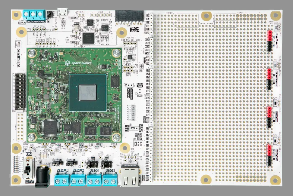
The SC-OBC Module A1 Development Board is designed to facilitate the user’s initial development of the SC-OBC Module A1. It incorporates the following interfaces necessary for software and FPGA development:
-
Flexible power interfaces, including a DC jack
-
Debug interfaces such as FPGA JTAG, PIC ICSP, and Zephyr Console
-
Communication interfaces including Controller Area Network (CAN) and User IO interfaces
Additionally, it features a Universal Area designed to facilitate the implementation of circuits built with User IO, aiding in initial system evaluation and BBM development.
|
The photograph shows pin sockets installed in the Universal Area, but they are not installed at shipment. Customers must solder the pin sockets themselves as needed for their evaluation environment. |